If you have ever wondered how a simple flat panel of glass and silicon can turn sunlight into electricity, you are asking one of the most fascinating questions in modern physics. The answer lies in a phenomenon called the photovoltaic effect—the physical process that allows solar cells to convert light directly into electrical energy without any moving parts, chemical reactions, or noise.
This guide will take you through the photovoltaic effect step by step, from the atomic level to the finished solar panel. By the end, you will understand exactly how sunlight becomes electricity and why solar cells have the efficiency limits they do.
1. The Photovoltaic Effect: What It Is and How It Was Discovered
The photovoltaic effect is the process by which light energy is converted into electrical energy in certain materials. It was first discovered by French physicist Edmond Becquerel in 1839, though practical solar cells made of silicon crystals were not developed until 1955. The first major application came in 1958 when silicon solar cell arrays became the primary power source for the Vanguard 1 satellite.
To understand the photovoltaic effect, you need to start with the material at the heart of every solar cell: the semiconductor.
2. Semiconductors: The Foundation of Solar Cells
2.1 What Is a Semiconductor?
A semiconductor is a material that conducts electricity only under certain conditions. Unlike metals, which conduct electricity freely, or insulators, which block it entirely, semiconductors sit in the middle. Silicon—the second most abundant element in the Earth’s crust—is the most common semiconductor used in solar cells.
In its pure form, silicon is a poor conductor. But when tiny amounts of specific impurities are added—a process called doping—its electrical properties change dramatically.
2.2 N-Type and P-Type Silicon
There are two types of doped silicon used in solar cells:
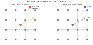
N-type silicon is created by adding a small amount of phosphorus (a fifth-column element). Each phosphorus atom contributes one free electron to the material, leaving behind a fixed positive charge. Because electrons carry negative charge, this type is called “n-type” (negative-type). Current in n-type silicon is carried by these free electrons.
P-type silicon is created by adding a small amount of boron (a column-three element). Each boron atom creates a hole—an absence of an electron—that behaves like a positive charge carrier. This type is called “p-type” (positive-type) because current is carried by these mobile holes.
2.3 The PN Junction: The Heart of the Solar Cell
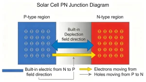
When n-type and p-type silicon are placed together, the boundary between them is called a PN junction. This junction is the most critical part of a solar cell.
At the interface, free electrons from the n-type side diffuse across to the p-type side, and holes diffuse in the opposite direction. This movement creates a region near the junction that is depleted of free charge carriers—the depletion region. The fixed charges left behind (positive on the n-side, negative on the p-side) create a permanent built-in electric field that points from the n-type side to the p-type side. This electric field typically measures about 0.5 to 0.6 volts and acts as a barrier that separates any charges created in the vicinity.
3. Step-by-Step: How Sunlight Becomes Electricity
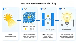
The conversion of sunlight into electrical energy involves three major processes:
3.1 Step 1: Absorption of Sunlight
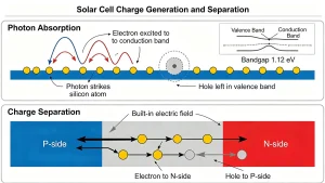
When sunlight strikes a solar cell, photons (particles of light) penetrate the surface and enter the semiconductor material. However, not every photon can generate electricity. A photon can only create an electrical charge if its energy is greater than the semiconductor’s bandgap—the minimum energy required to free an electron.
Silicon has a bandgap of approximately 1.1 to 1.12 electron volts (eV). Photons with energy below this threshold (primarily infrared light, which makes up about 30% of sunlight) simply pass through the cell without being absorbed. Photons with energy above the bandgap are absorbed, but the excess energy is lost as heat.
3.2 Step 2: Generation of Electron-Hole Pairs
When a photon with sufficient energy is absorbed by the silicon, it transfers its energy to an electron in the material. This energy “kicks” the electron from the valence band (where electrons are bound to atoms) into the conduction band (where electrons can move freely).
This leaves behind a hole—a missing electron in the atomic structure. The freed electron and the hole it left behind are together called an electron-hole pair. This pair represents the fundamental unit of electricity generation in a solar cell.
3.3 Step 3: Separation of Charges by the Built-in Electric Field
Once an electron-hole pair is created, the two charges must be separated—otherwise they will simply recombine and the energy will be wasted as heat.
This is where the PN junction’s built-in electric field comes into play. The electric field forces the negatively charged electrons to move toward the n-type side of the junction and the positively charged holes to move toward the p-type side. This separation of charge creates a voltage across the solar cell.
3.4 Step 4: Current Flow Through an External Circuit
The separated electrons and holes are collected by metal contacts on the front and back of the solar cell—the front grid lines and the back electrode. When these contacts are connected through an external circuit, the electrons flow through the circuit to power a device, then recombine with holes at the other end of the cell.
Each individual solar cell produces only about 0.5 to 0.6 volts. To achieve useful voltages for real-world applications, cells are connected in series within a panel. A typical residential solar panel contains 60 or 72 cells wired together.
4. From Photons to Power: The Big Picture
To summarize the entire photovoltaic process:
-
Sunlight (photons) strikes the solar cell.
-
Photons with energy above silicon’s bandgap are absorbed.
-
Absorbed photons create electron-hole pairs in the semiconductor.
-
The built-in electric field at the PN junction separates electrons and holes.
-
Separated charges are collected by metal contacts.
-
Connected to an external circuit, the electrons flow as direct current (DC) electricity.
This DC electricity is then sent to an inverter, which converts it to alternating current (AC) for use in your home or business.
5. Why Solar Cells Aren’t 100% Efficient
You might wonder: if the physics is so elegant, why don’t solar panels convert all the sunlight they receive into electricity?
The answer lies in fundamental physical limits. The Shockley-Queisser limit—a theoretical model published in 1961—sets the maximum possible efficiency for a single-junction solar cell at about 33%. For silicon with its 1.12 eV bandgap, the limiting efficiency is 33.4% under standard test conditions.
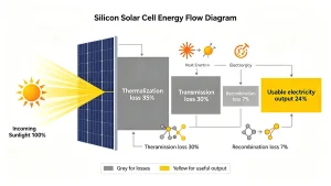
This limit exists because of three unavoidable losses:
-
Transmission loss: Photons with energy below the bandgap (about 30% of sunlight) pass through the cell without being absorbed.
-
Thermalization loss: Photons with energy above the bandgap (about 35% of sunlight) lose their excess energy as heat.
-
Radiative recombination loss: Some electron-hole pairs recombine before their energy can be collected.
In practice, commercial silicon solar cells achieve efficiencies of 18–24%,while cutting-edge laboratory cells have recently surpassed 28%. In May 2026, Trinasolar achieved 28.00% efficiency for a large-format crystalline silicon cell. Longi set a record of 28.13% for its HIBC solar cell in April 2026. These records represent steady progress toward silicon’s theoretical limit.
6. From Lab to Panel: How Efficiency Gains Reach Your Rooftop
The efficiency records achieved in laboratories do not immediately appear on residential rooftops. There is a significant gap between research-cell efficiency and commercial module efficiency. For example, while TOPCon cells have reached 26.9% efficiency in the lab,commercial TOPCon modules typically deliver around 24.1%. PERC technology, which was the industry standard just a few years ago, now tops out at 21.7% in commercial modules.
This gap exists because laboratory cells are made under perfectly controlled conditions with expensive processes that are not cost-effective for mass production. Manufacturers must balance efficiency gains against manufacturing costs, material usage, and production yields. Over time, however, the most promising lab innovations are gradually adapted for commercial production, driving steady improvements in the panels available to homeowners.
7. Bringing It All Together
The photovoltaic effect is a remarkable example of quantum physics applied to real-world problem-solving. By understanding how semiconductors, PN junctions, and light interact, we can appreciate both the genius of solar technology and its inherent limitations.
A solar cell is not magic—it is a carefully engineered device that harnesses the fundamental properties of matter to turn the sun’s energy into usable electricity. And with each passing year, researchers and manufacturers push closer to the theoretical limits of what silicon can achieve, making solar power cheaper and more accessible for everyone.